


FC1179主控芯片数据恢复参数如何解读?
| FC1179 AA2 2c 84 58 32 1x1 |
Layout
FC1178 1154_1150
Mix
Input
Order 0
Xor 21cd
Page 0x4000
Group 4
Divide
Field Block Number
Value 0x2ff
Add
Field Block Number
Value 0x30
Block Cut
Block 0x7B8000/0x4000/0x444000
Assembler
Block Number
Block Size 0xbfc000
Bank Space 0x4000
Image Cut 0x742000
Banks 00 / 0x000 / 0x0f4
Actions
Scan
Comments
For LBA pattern:
Very cool controller
Split by Block 4, 0xd9e000
For each split make separate image
Split order: 2,3,0,1
Join by Dump
In each split
need cut pages
Divide block number on (0x300 - number on cuted pages)
Need add some value to Block Number
And an Image Cut
Start of each image is missing
Have a fun :)
I give up on split_3
|
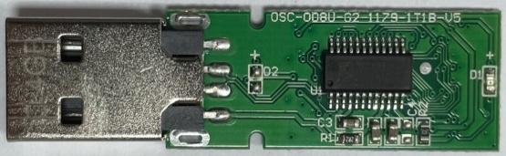
|
|
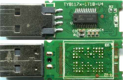
| |||
|
|
| FC1179 45 3c 98 b3 1x1 |
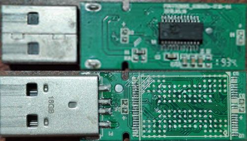
Layout
FC1178 1148_1144
Mix
Input
Order 0
Xor 21cd
Page 0x4000
Group 4
Block Cut
Block 0/0x30000/0xBA0000/0x30000
Divide
Field Block Number
Value 0x2e8
Add
Field Block Number
Value 0x11
Assembler
Block Number
Block Size 0xba0000
Bank Space 0x4000
Image Cut 0x5d6000
Banks 00 / 0x000 / 0x9ff
Actions
Scan
Comments
by Arvika
ID: 45 3c 98 b3 76 72
even blocks empty, odd with data
save disk.image, scan by any software
Check dirs ok
Possible rebuild full structure after additional work
Solution could be other if even and odd blocks have data
| FC1179 45 3c 98 b3 1x1 v2 |
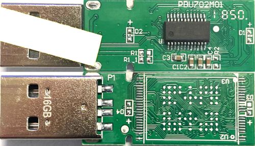
Layout
FC1178 1148_1144 v2
Mix
Input
Order 0
Xor 21cd
Page 0x4000
Group 4
Divide
Field Block Number
Value 0x2e4
Add
Field Block Number
Value 0x12
Block Cut
Block 0/0x38000/0xB90000/0x38000
Assembler
Block Number
Block Size 0xb90000
Bank Space 0x4000
Banks 00 / 0x000 / 0x9ff
Actions
Scan
Comments
by Arvika
ID: 45 3c 98 b3 76 72
To use this model need cut bad bits (if exist)
even blocks empty, odd with data
save disk.image, scan by any software
Check dirs ok
Possible rebuild full structure after additional work
Solution could be other if even and odd blocks have data
| FC1179 45 3c 98 b3 1x1 v3 |
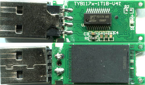
Layout
FC1178 1148_1144
Mix
Input
Order 0
Xor 21cd
Page 0x4000
Group 4
Divide
Field Block Number
Value 0x300
Add
Field Block Number
Value 0x62
Assembler
Block Number
Block Size 0xc00000
Bank Space 0x4000
Image Cut 0x800000
Banks 00 / 0x000 / 0x9ff
Actions
Scan
Comments
by Arvika
ID: 45 3c 98 b3 76 72
To use this model need cut bad bits (if exist)
save disk.image, scan by any software
Check dirs ok
Possible rebuild full structure after additional work
|
| ||||
|
|
| |||
|
|
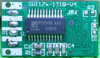
| FC1179 89 c4 08 32 1x1 |
Layout
FC1178 1154_1150 Xor e9e5_128
Mix
Input
Order 0
Divide
Field Block Number
Value 0x900
Assembler
Block Number
Block Size 0x2400000
Bank Space 0x4000
Banks 00 / 0x000 / 0x777
Actions
Scan
Comments
Serg for forum 12007
Verified only with Raw Recovery
11.04.2022 Divide changed
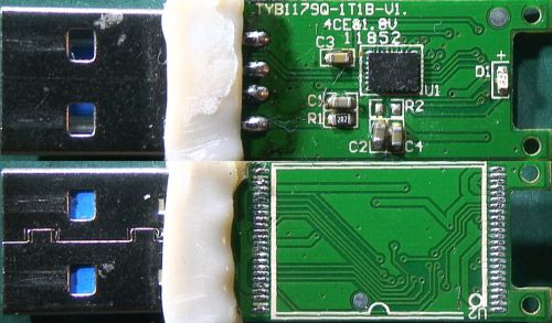
| FC1179 98 3e 98 b3 1x1 |
Layout
FC1178 1148_1144
Mix
Input
Order 0
Xor 21cd
Page 0x4000
Group 4
Block Cut
Block 0x11D0000/0x630000
Divide
Field Block Number
Value 0x8e8
Cross Block
Field Block Number
Block 0x11d0000
Parts 2
Step 1
Assembler
Block Number
Block Size 0x11d0000
Bank Space 0x4000
Mix 2 / 0x4000
Scan Max 1
Actions
Scan
Find Bank Size
Comments
by Arvika & Serg
Case use bad bits, first need remove them before use this model
RAW recovery
|
|
常见问题解答
FC1179芯片的闪存布局参数有什么特点?
FC1179芯片的闪存布局参数显示其采用1x1通道配置,Page大小为0x4000字节,Group分为4组,Divide Field块号值为0x2ff,Add Field块号值为0x30。这些参数决定了数据在闪存中的物理排列方式,对于取证软件正确读取和重组数据至关重要,尤其是在处理坏块或异常分区时,需要依据这些参数进行精确的地址映射。
如何处理FC1179主控的LBA模式数据恢复?
针对FC1179主控的LBA模式,文章建议采用按块分割策略:将数据按Block 4分割,每个分割块大小为0xd9e000,并按照2,3,0,1的顺序进行分割,然后通过Dump方式合并。每个分割块内还需进行页裁剪,具体操作是使用Divide block number减去裁剪页数(0x300),以确保恢复的数据完整且无冗余,适用于电子取证中的镜像制作。
FC1179芯片在取证软件中如何生成独立镜像?
在取证软件中,处理FC1179芯片时,需根据其Bank Space(0x4000)和Image Cut(0x742000)参数,将闪存划分为多个Bank(如00至0x0f4),每个Bank独立进行扫描和镜像。对于每个分割块,需先执行页裁剪操作,再按照指定的分割顺序(2,3,0,1)生成独立镜像,最后在Dump阶段按顺序合并,确保镜像的连续性和可验证性,满足司法鉴定对数据完整性的要求。