


AU8910芯片数据恢复怎么做?
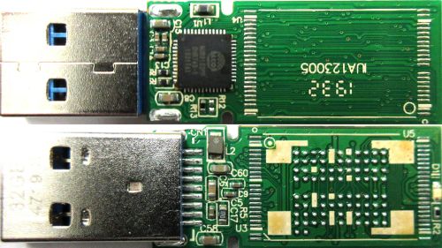
| AU89102DF 2c 84 58 32 1x1 |
Layout
AU8910 1152 Xor 6771_256
Mix
Input
Order 0
Block Pair
Block 0xc00000
Page 0x4000
Assembler
Block Number
Block Size 0x1800000
Bank Space 0x4000
Banks 00 / 0x000 / 0x2e3
Actions
Scan
Comments
Serg for forum 12142
|
|
| AU89102DF 2c c4 18 32 2x1 |

Layout
AU8910 1152 Xor 6771_1728_256
Mix
Input
Order 1/0
Block Pair
Block 0x5100000
Page 0x4000
Join by Dump
Parts 2
Assembler
Virtual Translator
Block Size 0xa200000
Comments
by Arvika
MBR need rebuild manually
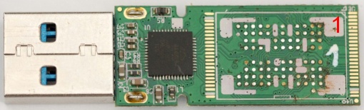
| AU89102DF 2c c4 18 32 2x1 v2 |
Layout
AU8910 1150 Xor 6771_1728_256
Mix
Input
Order 1/0
Software Bad Bytes
Block 5184
Group 1
Block Pair
Block 0x5100000
Page 0x4000
Cross Bank
Block 0xa200000
Bank 0xe7
Join by Dump
Parts 2
Assembler
Block Number
Block Size 0xa200000
Bank Space 0xe7
Image Cut 0x40000
Actions
Scan
Find Bank Size
Comments
Serg for forum 11979
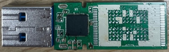
| AU89102DF 2c c4 18 32 2x1 v3 |
Layout
AU8910 1152 Xor 6771_1728_256
Mix
Input
Order 1/0
Block Pair
Block 0x5100000
Page 0x4000
Cross Bank
Block 0xa200000
Bank 0xe7
Join by Dump
Parts 2
Assembler
Block Number
Block Size 0xa200000
Bank Space 0xe7
Actions
Scan
Find Bank Size
Comments
Serg for forum 12270
|

|
| AU89103-AA1 2c c4 18 32 1x1 |

Layout
AU8910 1152 Xor 6771_1728_256
Mix
Input
Order 0
Block Pair
Block 0x5100000
Page 0x4000
Cross Bank
Block 0xa200000
Bank 0xe7
Assembler
Block Number
Block Size 0xa200000
Bank Space 0xe7
Actions
Scan
Comments
Serg for forum 11984
Tested with Raw Recovery
I do not make Check Dirs
| AU89103-AA1 2c c4 18 32 2x1 |

Layout
AU8910 1162 Xor 6771_0x6c0_256
Mix
Input
Order 1/0
Block Pair
Block 0x5100000
Page 0x4000
Block Pair
Block 0xa200000
Page 0x8000
Join by Page
Parts 2
Page 0x10000
Assembler
Raw
Comments
Serg for forum 12851
Can not build VT
Each top dir have alot of updates
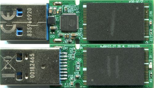
| AU89103-AA1 89 c4 08 32 2x1 |
Layout
AU8910 1162 Xor 6771_256
Mix
Input
Order 1/0
Block Pair
Block 0x2400000
Page 0x4000
Block Pair
Block 0x4800000
Page 0x8000
Join by Dump
Parts 2
Assembler
Block Number
Block Size 0x9000000
Bank Space 0x4000
Image Cut 0x8000
Banks 00 / 0x000 / 0x3bc
Actions
Scan
Comments
by Arvika
dump order can be other
structure was borken, need rebuild.
| AU89103-AA1 98 3c 98 b3 1x1 |
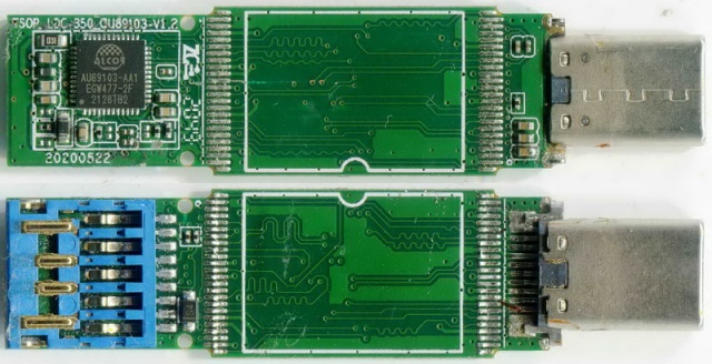
Layout
AU8910 1146 Xor 6771_384_256
Mix
Input
Order 0
Block Pair
Block 0x1800000
Page 0x4000
Block Cut
Block 0x2400000/0xC00000
Assembler
Block Number
Block Size 0x2400000
Bank Space 0x4000
Banks 00 / 0x000 / 0x3ff
Actions
Scan
Comments
Serg for forum 12806
常见问题解答
AU8910芯片的数据提取参数是什么?
根据文章,AU8910芯片的数据提取参数包括:ID码为2c 84 58 32,Layout为AU8910 1152 Xor 6771_256Mix,Input Order为0,Block Pair Block为0xc00000,Page为0x4000,Assembler Block Number为0x1800000,Bank Space为0x4000,Banks为00/0x000/0x2e3。这些参数用于取证软件中正确配置芯片读取流程。
AU8910与AU6989在提取时有何不同?
文章提到,AU8910的Layout为AU8910 1152 Xor 6771_256Mix,而AU6989的Layout为AU6989 1152 Xor 6771_256Mix。此外,AU8910的Block Pair Block为0xc00000,Page为0x4000,而AU6989的Block Pair Block为0x2400000,Page为0x4000,且AU6989需要Assembler Virtual Translator,Block Size为0x4800000。两者参数不同,需分别配置。
AU8910提取时速度慢怎么办?
文章建议,对于AU8910芯片,如果提取速度慢,可以尝试运行自动慢速模式,然后再运行自动快速模式,或者手动重建虚拟翻译器(VT)。具体操作需根据实际软件界面和芯片状态调整,以确保数据完整读取。